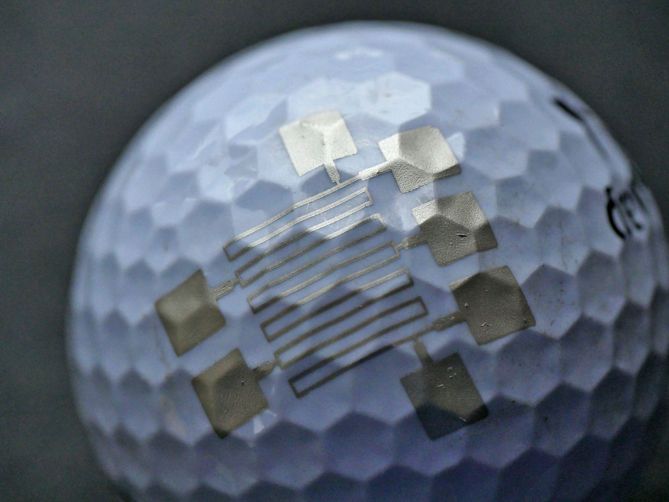
Sensors printed directly onto the workpiece
Our aim is to break new ground in printing technology. The printing system developed by binder, the binder method, allows functional layers, such as electrodes or conductor tracks, to be applied directly to three-dimensionally shaped or structured surfaces. This method is suitable for substrates such as plastic, metal, glass, ceramics and much more.
- Force sensors and strain measurement
- Capacitive touch fields
- Heating elements
- Printed conductor tracks
- Elektroluminescence (printed lights)
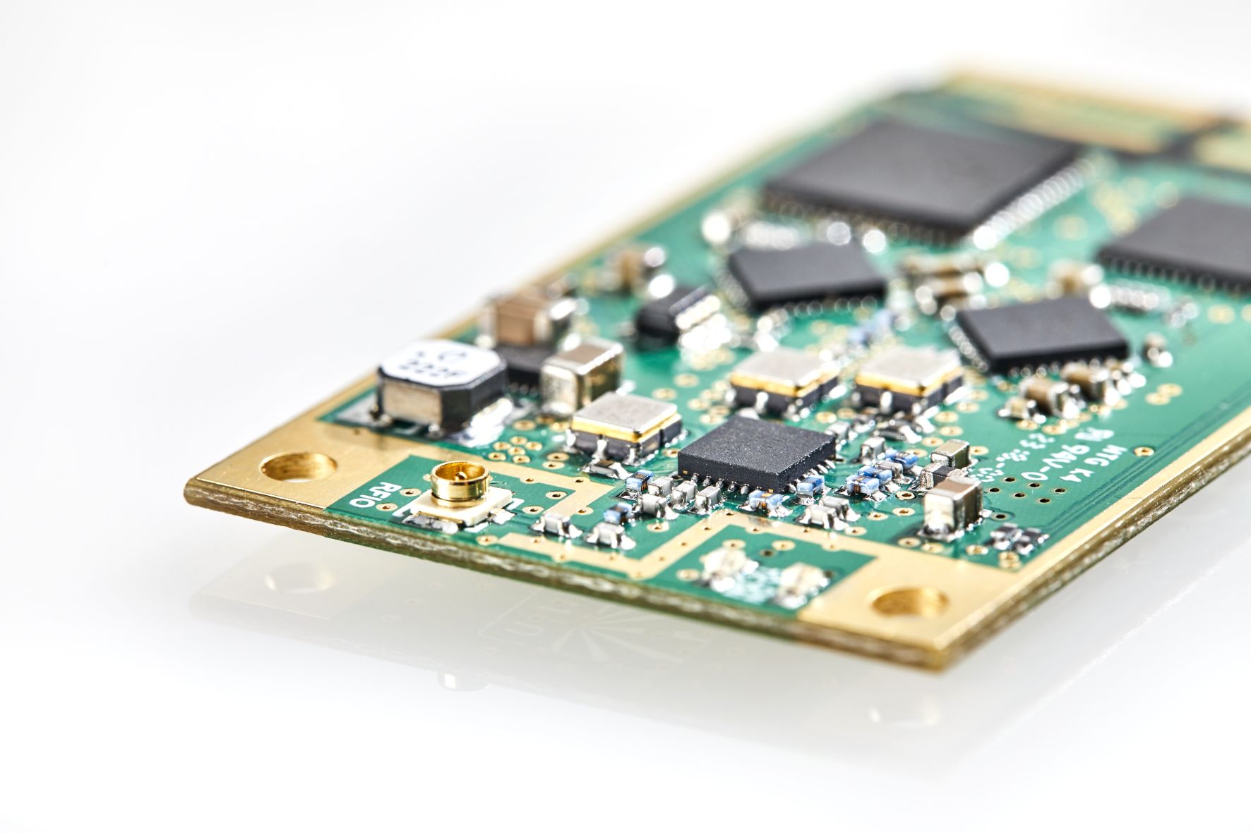
From the idea to the finished product
Electronics development is in the best hands with us right from the start. From conceptualisation and circuit design to planning series production, binder electronic solutions offers complete solutions.
- Customised solutions
- Project management
- Electronics development and circuit layout
- Software engineering
- Support through to serial production
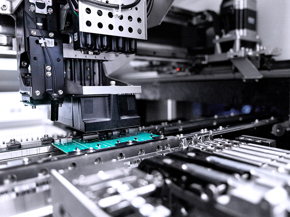
Express service and sample production – fast and competent
Things have to happen quickly during development. Thanks to binder electronic solutions‘ good location distribution, we are close to our customers and can react flexibly to customer requests.
- Express service for components / assembly
- Prototypes, sample and small series production
- Modification and repair service
- Consultancy for production-ready design
- Certified according to ISO 9001:2015, 14001
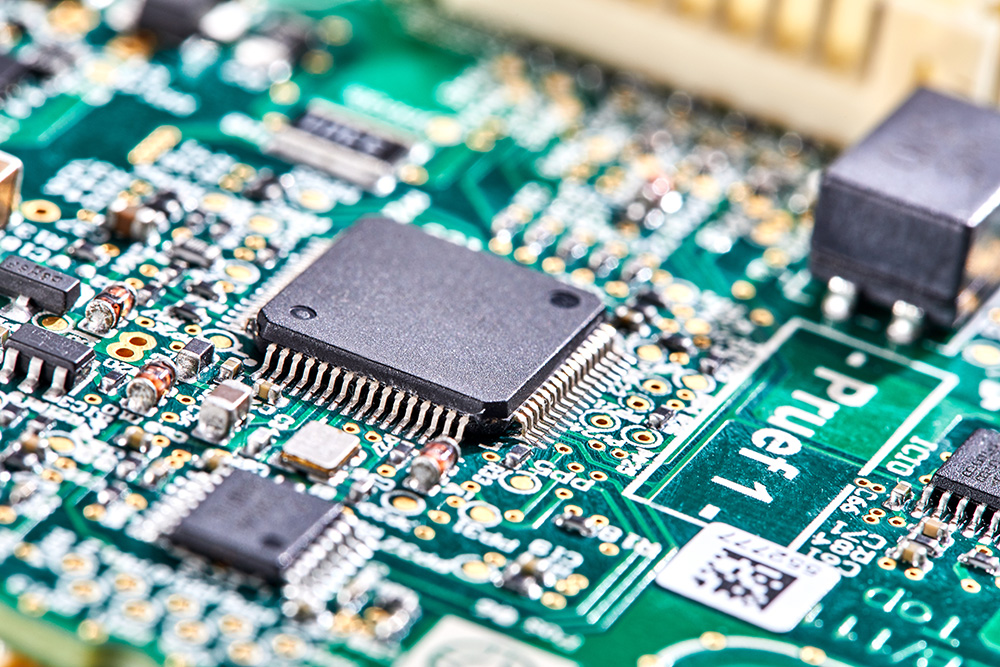
Reliable, economical and local
We offer direct integration into our customers‘ value chain. This enables us to guarantee punctual and smooth delivery in impeccable quality, even when our customers‘ requirements change.
- Component procurement
- SMD line production incl. 3D AOI testing
- Soldering processes using reflow soldering, wave soldering and selective soldering
- Electrical testing and ICT
- Cleaning, painting and moulding of electronic assemblies